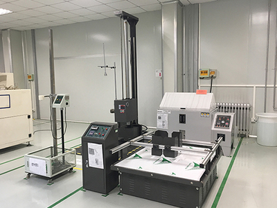
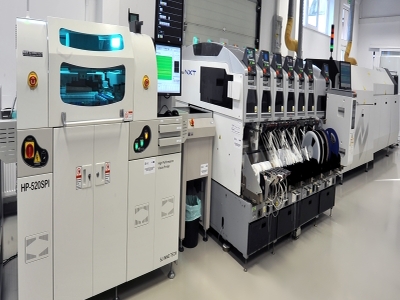
Manufacturing & Technology
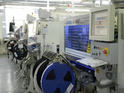
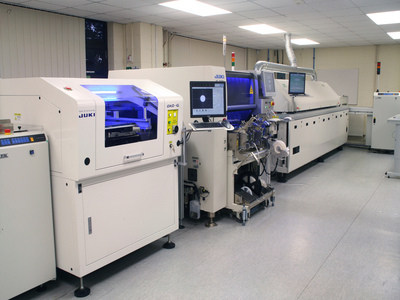
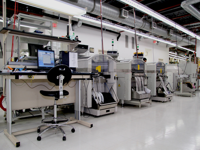
Overview of the factory
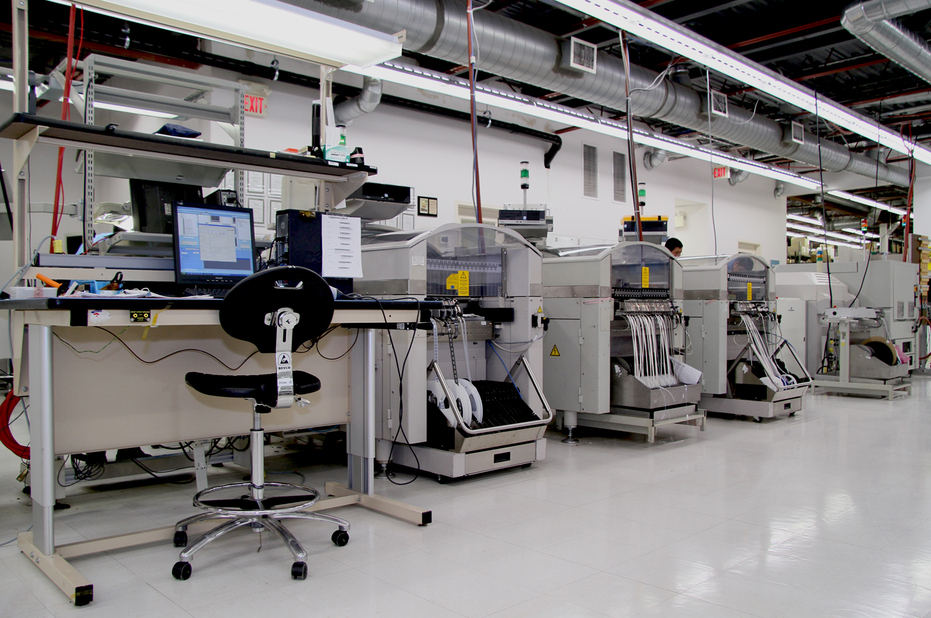
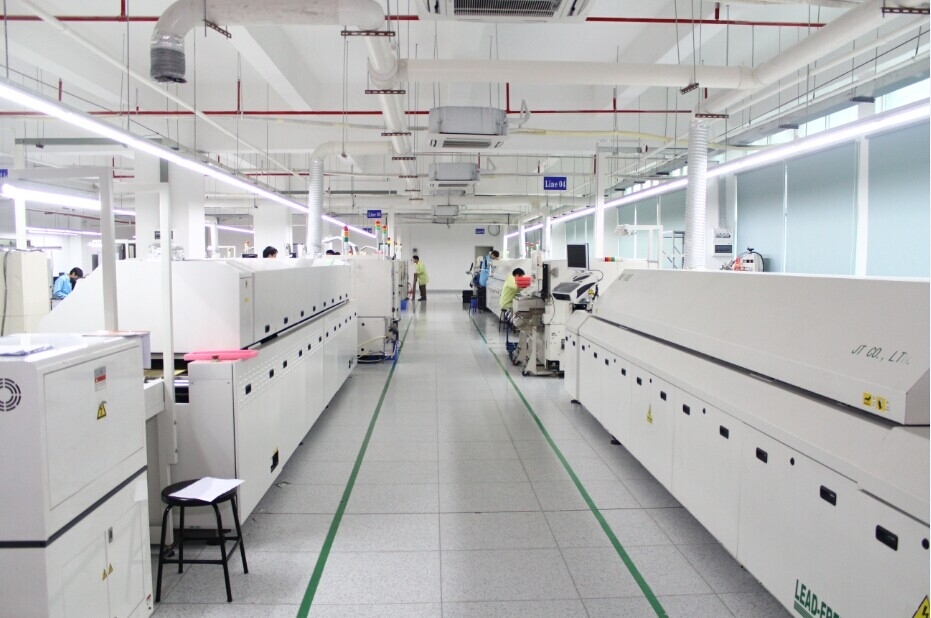
Rigid PCB Capabilities
| Materials | FR4, High TG FR4, Halogen Free Material, CEM-3. Rogers HF Material, Aluminum |
|---|---|
| PTFE Laminates | Rogers series, Taconic series, Arion series, Nelco series, Nelco series, Taizhou Wangling F4BK series, TP series |
| Hyrid Laminating | Rogers/Taconic/Arion/Nelco laminate with FR-4 material – including partical RO4350B hybrid laminating with FR-4 |
| Layers | 1 – 64 layers |
| Board Thickness | 0.1 – 10 mm |
| Slodermask Type (LPI) | Kuangshun, Taiyo, Himonia, Nanya, Onstatic, Chung Yu, MSDS |
| Soldermask Color | Green, Yellow, Black, Blue, Red, White, Purple, Orange, Matte green, Matte blue, Matte black |
| Surface Treatment | HASL, HASL-LF, OSP, ENIG, ENEIPG, Hard gold, Gold finger |
| Min.Line / Track Width | 3 mil |
| Min.Mechanical Drill Hole | 0.10 mm |
| Min.Drilling Slot Size | 0.6 mm |
| Copper Thickness | 20 oz MAX |
| Legend / Silkscreen Color | Black, White, Yellow and others |
| Other Technology | Peelable Mask, Carbon ink, Non-across Blindried Vias, Characteristic Impedance Control, VIA IN PAD, etc |
| HDI | 1 + N + 1, 2+ N + 2, 3 + N + 3, Anylayer HDI |
| Buried & Blind via | 4 – 64 layers, 0.5 – 10 mm (Board Thickness) |
Rigid-Flex PCB Capabilities
| Flex & Rigid-Flex PCBs | 1 -10 layers Flex PCB & 2 – 20 layers Rigid-flex PCBs |
|---|---|
| FCCL (adhesive) | Shengyi SF305, PI = 1 mil and 2 mil, Cu = 0.33 oz & 0.5 oz & 1 oz Panasonic R-F5775(ER), PI = 1 mil and 2 mil, Cu = 0.33 oz & 0.5 oz & 1 oz Dupont Pyralux AR PI = 1 mil and 2mil, Cu = 0.5 oz & 1 oz |
| Coverlay | Shengyi SF305C & 0515 & 0525 &1025& 2030; Talflex FHK 1025 & 1035 |
| NO FLOW PP | Ventec: vt-47n(TG170) & em-285b(TG150) |
| CCL | ITEQ: IT180A Shengyi: S1000H & S1000-2 Arlon: 85N Nelco: N4000-13 series |
| Board Thickness | 0.3 – 3.0 mm |
| Board Size | 10mm * 15mm Min 406.4mm * 558.8mm Max |
| Min. BGA pad size | 12mil (8mil for electrical soft gold board) |
| Surface Treatment | HASL, HASL-LF, ENIG, ENEPIG, Hard Gold, Immersion silver. Immersion tin, OSP |
| Bow & Twist | 0.75% (symmetrical) |
| Other Techniques | HDI Gold Fingers Stiffener (Only for PI / FR4 Substrate) |
HDI ( High-Density Interconnect)PCB Capabilities
| Feature | Capacity |
|---|---|
| HDI PCB type: | 1 + n + 1, 1 + 1 + n + 1 + 1, 2 + n + 2, 3 + n + 3 (n buried vias ≤ 0.3 mm) |
| Blind&buried via type: | mechanical blind & burried vias with less than 2 times laminating; Laser blind via |
| Min laser drilling size: | 4 mil |
| Max laser drilling size: | 6 mil |
| Finshed mechanical hole size: | 5-244 mil (corresponding drilling tool size 8-248 mil) |
| Max aspect ratio for hole plate: | 10 : 1 |
| Max aspect ratio for laser via filling plating: | 0.9 : 1 (Dpeth included copper thickness) |
| Min gap between hole wall and conductor (None blind and buried via PCB): | 7 mil (≤8L), 9 mil (10-14L), 10 mil( > 14L) |
| Min gap between hole wall conductor (Blind and buried via PCB): | 8 mil (1 times laminating), 10mil (2 times laminating), 12 mil (3 times laminating) |
| Min gab between hole wall conductor (Laser blind hole buried via PCB): | 7 mil (1 + N + 1) ; 8 mil (1 + 1 + N + 1 + 1 or 2 + N + 2) |
| Min space between laser holes and conductor: | 6 mil |
| Min space between hole walls in different net: | 10 mil |
| Min Pad size for laser drillings: | 10mil (for 4 mil laser via), 11 mil(for 5 mil laser via) |
| Min Pad size for mechanical drillings: | 16 mil (8 mil drillings) |
The Different Types Of HDI PCB Structures
With the capacity to produce HDI PCBs of up to 32 layer,depending on the unique requirements of each project. Below is a table outlining the different types of HDI PCB structures we can create.
| HDI PCB Structures | The Various categories of Micros Vias | Large-Scale Production | Small to Medium-Scale Production | Prototype | Available |
|---|---|---|---|---|---|
| 1 + N + 1 | Blind vias | Yes | Yes | Yes | Over 4 layers |
| 2 + N + 2 | Blind/Buried staggered vias | Yes | Yes | Yes | Over 6 layers |
| 2 + N + 2 | Blind/Buried stacked vias | Yes | Yes | Yes | Over 6 layers |
| 3 + N + 3 | Blind/Buried stacked vias | / | Yes | Yes | Over 8 layers |
| 3 + N + 3 | Blind/Buried stacked vias | / | / | Yes | Over 8 layers |
Advanced Equipments Show
